


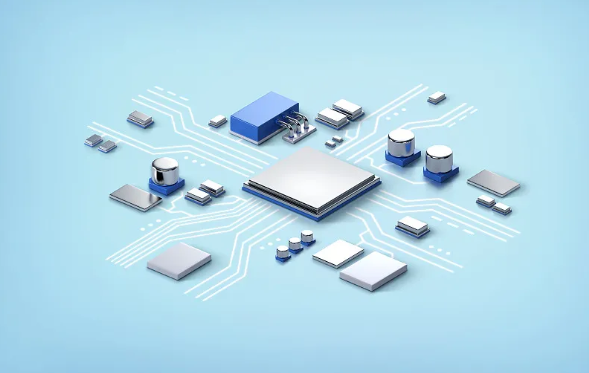
电路板被描绘成一个矩形形状,其表面充满了精细的线条
The circuit board is depicted as a rectangular shape, and its surface is full of fine lines and patterns, representing the various components and connections on the circuit board These elements, including resistors, capacitors, transistors, and so on, are drawn very finely so that we can see their shape and position clearly On one side of the circuit board, we can see a flattening tool that looks like a large scraper or roller that is flattening the surface of the circuit board The process is depicted so vividly that we can see that some of the widgets on the surface of the circuit board are being flattened while others remain intact At the bottom of the model diagram, there are some text and arrow annotations that explain the specific steps and principles of the flattening process These annotations are very detailed, allowing us to better understand the process In general, this model vividly depicts the process of chip semiconductor circuit board flattening, allowing us to

描述你想生成的图片信息,如:画面里有什么风格/元素/色彩
Shift+回车 = 换行
AI可能会犯错误或不完全遵循,请谨慎使用。
同款 0
评论 0